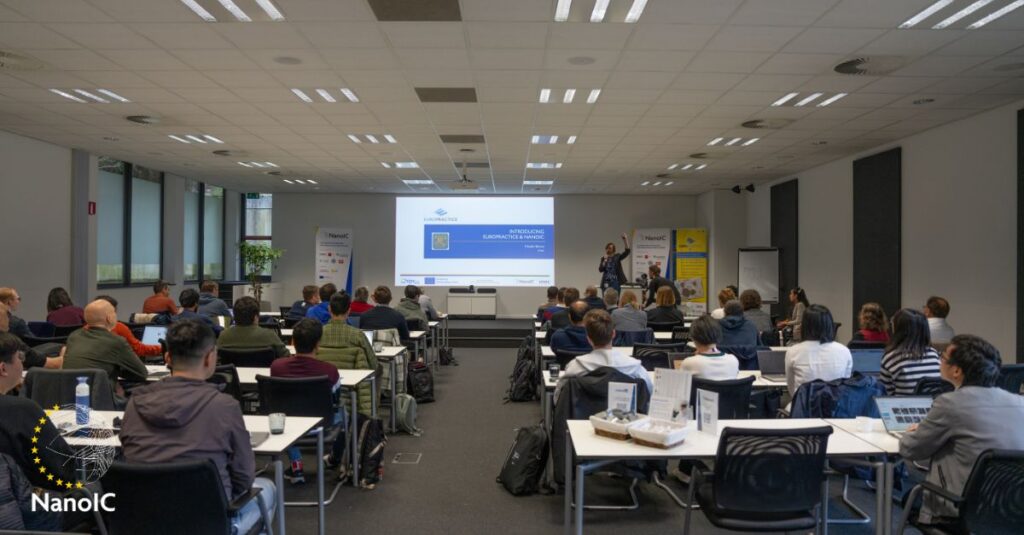
The Estonian Chips Competence Centre (KIIP) participated in the Advanced PDK Workshop: N2 and A14 Nanosheet Pathfinding and Applications, organised by imec in collaboration with Europractice and the NanoIC pilot line. The event brought together European chip competence centres, research organisations, and industry partners to explore emerging design technologies beyond the 2nm node.
The workshop focused on pathfinding Process Design Kits (P-PDKs) for advanced CMOS technologies, providing participants with both theoretical insights and hands-on experience in next-generation chip design environments.
Advancing design capabilities for future nodes
A key focus of the workshop was the use of pathfinding PDKs, which enable early-stage experimentation with technologies that are not yet available in production. These environments allow designers to evaluate architectures, validate concepts, and explore trade-offs well before fabrication becomes possible.
Participants worked with advanced design flows and tools, gaining exposure to:
- Nanosheet (gate-all-around) transistor architectures
- Backside power delivery networks
- Advanced digital design flows and toolchains
- Design-technology co-optimization (DTCO) approaches
This reflects a broader shift in the semiconductor industry, where innovation increasingly begins at the design stage, supported by realistic yet forward-looking modelling environments.
Key insights for the European chip ecosystem
The workshop highlighted several important trends shaping the future of semiconductor development in Europe.
First, early access to advanced design infrastructure is becoming a critical competitive factor. Pathfinding PDKs allow organisations to prepare for future nodes years in advance, reducing development risks and accelerating innovation cycles.
Second, new device architectures such as nanosheet transistors and backside power delivery are emerging as standard building blocks for sub-2nm technologies, enabling improvements in performance, energy efficiency, and design density.
Third, the importance of design-technology co-optimization (DTCO) continues to grow. Future competitiveness will depend on the ability to co-develop circuits and process technologies in parallel, rather than sequentially.
Finally, initiatives such as NanoIC are contributing to the democratization of advanced chip design, making leading-edge capabilities accessible to a wider range of organisations, including startups and research institutions.
Relevance for Estonia
For Estonia, participation in this workshop supports the development of a design-driven semiconductor capability, aligned with the goals of the European Chips Act and the broader competence centre network.
Access to advanced PDK environments enables Estonian stakeholders to:
- Engage with next-generation technologies at an early stage
- Develop high-value design expertise and intellectual property
- Strengthen collaboration with leading European partners
- Integrate more effectively into international semiconductor value chains
As KIIP continues to support companies in chip design and pilot production, such activities play an important role in building the skills, knowledge, and partnerships required for long-term competitiveness.
Strengthening Estonia’s position in the European ecosystem
The workshop further reinforces KIIP’s role as a gateway for Estonian companies and researchers to access European-level infrastructure, expertise, and collaboration networks. By connecting local actors with initiatives such as NanoIC and Europractice, KIIP contributes to the growth of a knowledge-based and innovation-driven chip sector in Estonia.
Participation in international workshops and pilot line activities is an important step in ensuring that Estonia remains aligned with the latest technological developments and can actively contribute to Europe’s semiconductor future.
Looking ahead
The insights and experience gained from the workshop will be used to support KIIP’s ongoing activities in capability building, training, and industry collaboration.
As semiconductor innovation increasingly shifts toward early-stage design environments, Estonia has a clear opportunity to position itself as a high-value contributor in advanced chip design within Europe’s evolving ecosystem.